Trial run lab course

Aside of conducting my research, I have a duty work as a lab assistant for one course work per semester. At the beginning I thought my involvement in this activity will bother me a lot. In fact, I kind of enjoy it.

A pastor in Baptist Church, to whom I usually update what I have been doing in the university, my current general research status, told me once, “that is great, now you have a chance to take a break. Reading a bit, planning for the next experiment and execute it confidently”. For some reason, his words relieve my stress.

What I am looking forward this semester is assisting student doing their coursework. Of course I have legal reason to get out from my office or else I have to sit the whole day in there, most likely with wandering mind if I can’t focus reading. Being with the students also interests me a lot. I can interact with them, showing them something, teaching them what I have learnt before them. I know at some point that they will surpass me and no surprise from my side, as they are the best mind that Norway has at the current moment.

Lab course will be officially started next Monday. I have schedule on Monday, at 8 AM. So, in order to make the lab session fruitful and lively with the student, I and other three lab assistants have conducted trial and run on two first module. We did it yesterday for lithography part and today for scanning electron microscopy (SEM)-energy dispersive x-ray spectroscopy (EDS) part.

Most of the steps I went through for this labwork are the same with the labwork this spring. In here, the teaching assistant basically will show them the basic guidance how to do proper work, and then licensed will be given to them once they pass. After that, they will do their own work, based on the objectives that we have set for them. This labwork will train them to be an independent researcher! Cool!

For the trial and run, since we were not able to find the mask specifically designed for this course, we used the one from the labwork last semester. The rest are exactly the same. It took place in Student lab in Nanolab. We did scribbing, then it is continued to cleaning+dehydration, coating, soft baking, exposing, developing and inspecting the sample; These steps are typical for conventional photolithography. Oh yes, we skipped post exposure bake and hard bake. If my memory serves correctly, we did not do post exposure bake and hard bake due to the datasheet for the negative photoresist we used, does not require these steps.

Some mistakes were done during this lab session. In the scribbing part, we spent quite some time to split the 2-inch Si wafer properly with 111 direction.
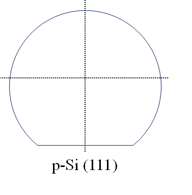
Picture 2-inch Si (111) wafer and the scribber direction

It is not easy :p

Errors during the photolithography steps were unavoidable: fallen sample, flipped sample with applied photoresist on it. But overall, it was fun 😀

We spent like three hours in total to do the step. The main problem was the produced samples (three in total) were not developed completely even after waiting time for about 10 minutes. The reason can be the expired photoresist or expired developer. Since we will not measure electrical properties of our sample, spots laying around on the channel are not problem. Nevertheless, I will do strict examination so that they have such kind of habit when they are working indepently. Ah, the geometry that we are aiming is Hall bar.
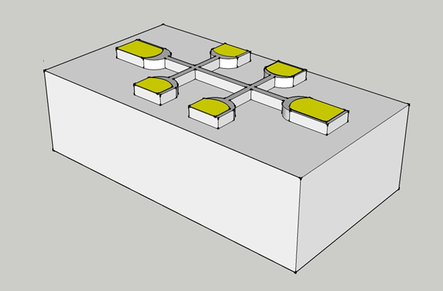
Picture Hall bar
Picture Hall bar

The processed samples were then brought to SEM for geometry inspection, focused especially on the cross section where the undercut pattern is checked. Once they were imaged, the last characterization was done using EDS. This technique can tell us what kind of elements are building up in specific area of the imaged sample. With EDS, we can get information whether we have correct deposited materials on the sample… or not.

Honestly, we had a struggle during elemental mapping using EDS technique. Theoretically, no matter what the size of the analysis area is, it should give what it should be. We had elements which were not supposed to be there, aside of other elements which were successfully mapped correctly. Let’s say we have image as illustrated like this:
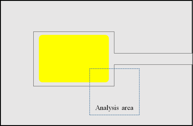
Illustration with rectangular and analysis area

Based on the image, we have metal on top of the GaAs sample. The metal itself should be consisted of, for example: Ge/Ti/Pt/Au where Au being the thickest part (200 nm) while Ge, Ti and Pt are around 20 nm, each. The EDS show expected Ga and As mapping where its concentration are more intense (indicated with more words of “Ga” and “As”) in the outside of the metal contact.
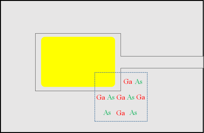
Illustration with rectangular and analysis area, Ga and As

In the metal contact itself, we had Pt and Au elemental mapping at the correct position.
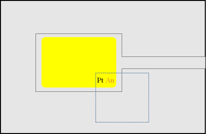
Illustration with rectangular and analysis area, Pt and Au

Unexpected results we got from the two most bottom layer of the metal: Ge and Ti, where they appeared not only in the metal contact, but outside as well. Even more, it looks like the concentration of Ge was lot stronger in the outside area than in the contact.
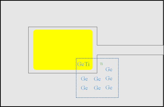
Illustration with rectangular and analysis area, Ge and Ti

After discussion with friend, a suggestion come to use smaller analysis area. Beside larger spot size of the incoming electron, the reason is the scattering of the x-ray signal passing through other parts of the sample, illustrated as rough sketch below (size is not scaled).
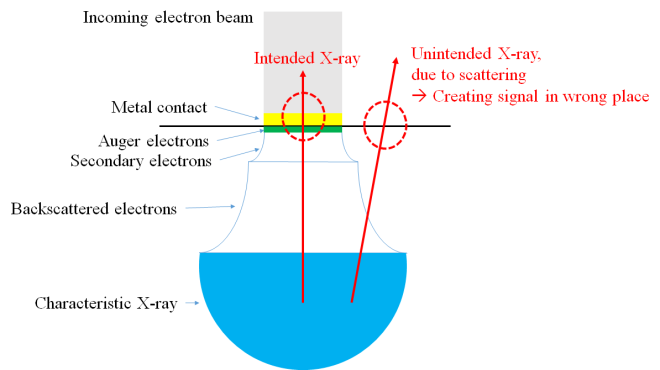
SEM signal + scattering

The results were much better than the previous one with larger analysis area. Each of the registered elements sit in the place where they should be sitting. Especially for Ge, more intense signal came from it with smaller analysis area. The only drawback was that, we cannot image the transition border between the metal and substrate at the same time. If we had done this, the same result would have appeared like the one before. The only thing that can be done were imaging one part standing close to each other, and makes an analysis of them separately.
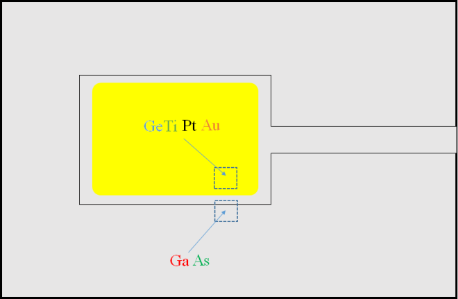
Illustration with rectangular and smaller analysis area, Ge/Ti/Pt/Au and Ga/As

I am not sure whether this is a correct approach or not. Any suggestion and thought are welcome!
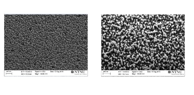
Well, it is a nanowire!

No nanowire growth has been done this week. Since there are two of my friends planning to use MBE with nitrogen-free chamber next week, the engineer decided to let growth chamber of MBE in the idle state or no nitrogen-related growth takes place for two-three days. Based on his experience, the decided recovery time is supposed to be sufficient enough to get nitrogen away from growth chamber, indicated from the pressure as low as 10E-10 or even lower. It means the growth chamber is in the ultra high vacuum state. The reason is because of my friends will grow in arsenic rich condition where the presence (even the small portion) of nitrogen is not desirable. Even with small portion of nitrogen, the growth sample will have diluted-nitride on it, a well-known method to alter energy band-gap of semiconductor.

No growth means characterization. I brought few of the grown samples to the scanning electron microscopy laboratory in the material department. I went training two weeks ago and did some two measurements where the results are not well-adjusted, according to my friends who has expertise in this area. In order to fix my weakness, I asked them, not once but twice to come with me but of course with different persons as I know they have their own work. Well, I think my efforts are fruitful in the sense of achieved better resolution image resulted from less distortion from astigmatism, focus and aperture optimization. Some tips and tricks were given to me , such as finding the beam location, the proper working distance (it is not in-lens type), in-plane and out-plane stage rotation.

I learned scanning-tunneling electron microscopy in Nanolab. It is bit different than the one in the material department where a transmission can be done in the same machine. Of course there is a dedicated machine to do transmission electron microscopy. As a result, such a small sample is required before it is loaded into the sample holder. I am impressed with this machine because it has way much faster venting and pumping time owing to the small chamber volume compared to the scanning electron microscopy in the material department. One of my friend always jokes that in order to get the machine in high vacuum, the user has to pay 75-100 NOK. In addition, scanning-tunneling electron microscopy in the Nanolab uses in-lens objective lens meaning the users do not have to bother much adjusting working distance as this parameter is the fixed value. With this type of lens, the resolution can go down to 0.5 nm but the drawback is located in the very limited sample size. Overall, both machine has similarities.

To use this wonderful machine, there is a theory, practical, self-training and examination part that I had to participate and pass. Generally, I did not have any difficulty in adapting with this machine. Just… The way of removing and inserting the sample holder is new for me. I have to rotate a bit, pull, rotate all the way, pull again, press “Air” button. The same method with opposite direction when I have to put it back. In one occasion of inserting the sample holder, after “Vac” button was press, I forgot to wait until the LED blink. I just force it to rotate and as a result, an alarm was beeping >_< I just realized my mistake after 5 minutes :p During this time, I was really afraid that I broke the machine XD

I showed my scanning electron microscopy images to the one who assisted me growing the first 7 samples. I suggested that no nanowire was observed in these samples, even with the help of AlN buffer layer. Before meeting with him, I knew that he would be disappointed with these results. Surprisingly, he did not show that sign at all and said that those short things were actually the nanowire, especially his own growth! Well, those words are in fact what I needed for the efforts we have put in the first attempts of GaN nanowire growing. Though they were not properly forming as a nanowire due to its short length. He suggested that the next growth with higher nitrogen flow. I am thinking to grow with much longer time, probably 2-3 times than what I did in the last 7 samples.

As for the last growth, I used double Ga flux rate to confirm whether the nanowire will increase its height by double. It did not turn to the expectation. It had the same height approximately with the the others. Of course, as the Ga flux was doubled, the physical mechanism on GaN nanowire formation was slightly changed. For instance, the edge has more two dimension growth (see picture below) resulting in higher non-uniformity toward the center. What a bad sample unfortunately, but I learned something at least. Maybe a lower growth rate can be planned as well? Such extreme growth rate was done by Galopin et al, almost half of the assigned Ga flux rate I set.

Growth comparison between double (left) and normal Ga flux rate (right). Two dimensional film is dominating in the left picture

Further GaN growth experience with MBE

Another two weeks, from the last week of July to the first week of August were scheduled with the attempt to grow nanowire structure of GaN material on the substrate of Si. There were five samples in total I could grow within these period. Considering the normal workload, the number of grown samples were quite normal.

I think I will not have any growth chance for the next 3-4 weeks ahead, since there are other person who also will use this MBE requiring different chamber condition. That is why the MBE system need to be stabilized for some time, 2-3 days before a cleaning and purifying stage are conducted from Nitrogen environmental condition.

I was thinking to grow two-three samples each day last week. But I guess it was impossible to do, since the growth itself took 3 hours added with another 2-3 hours calibrating the flux of the source, outgassing the sample and preparing the chamber in such way to favorably grow in suppressed contaminated environment which can destruct the growth of GaN. Moreover, I am not confident enough and officially not allowed to transfer substrate from one chamber to another, or else I mess up with the machine. Fallen substrate holder in any chamber is not really good idea, since the engineer has to vent the chamber, pump back to vacuum, bake the chamber to remove the contaminants-oxides and another source calibrations here and there. Believe it or not, this sequence will take around 3-4 weeks. That is why I do not want to mess up. Simple reason why I can’t grow more than one sample is because of the available substrate holder for the 2 inch wafer is only one. Well, at the same time I am relieved.

Normally, I start ramp down the load-lock chamber at 9 AM. While it is ramping down, I calibrated the required source fluxes to be met at certain number so that it equivalents to the growth rate I want. Well, It takes like one hour. Then my friend helped me to transfer the sample from load lock chamber to heater station located in buffer chamber. Another hour spent to let the sample heated to remove any possible contamination, until the pressure is low enough. Finally the sample is transferred from buffer chamber to growth chamber. Yet the growth can’t be started directly. The real outgassing is done in the growth chamber. Why is it real? Because this process undergoes very high temperature up to 900 °C. It can’t be done in the buffer chamber, as the highest temperature is limited up to 600 °C. It is taken to avoid As evaporation on the substrate holder which has been used previously with the As based sample or growth. The evaporated As atoms can make the viewport to be darkened, making the grower can’t really see and therefore disturbing the transfer process. While in the growth chamber, not much to be seen and it is ok to let the outgassing being done in the very high temperature.

Outgassing process itself takes time and once more, very low pressure or good vacuum pressure indicates less and less contamination exist on the surface of the sample. Once it is done, then the growth can be started. Generally, these steps are the same for all typical growth using MBE, no matter what substrate and kind of structure. One thing to remember is that the different sample may undergo different outgassing temperature. For instance GaAs substrate must not exceed than 650 °C to avoid evaporation of As even in the As chamber condition. Without As help, the temperature for GaAs must not exceed more than 400 °C. If it being done, the sample will be ruined even before the growth has not started.

Now what I did for the past two weeks actually can be divided into two different methods. First was directly grown on Si and the second part was helped by buffer layer of Al. The first growth was exactly similar with the previous weeks with the differences in the nitridation treatment and growth temperature. The reasons for changing these two growth conditions were to put more nitrogen incorporation in the nanowire structure and further increase the probability of getting nanowire structure instead of thin film. Well, after scanning electron microscopy measurement, I had a feeling of what the nanowire looks like, better than the last growth but the problem located on how short the grown nanostructure was. The growth time was almost two and half hours, but the height was less than 200 nm where I expected to be at least 400 nm.

Then at the second growth, as my friend suggested me that using Al deposition forming AlN after nitridation can increase the probability of getting nanowire structure, way much better than directly on bare Si. There are many reports using this method and one example is by Songmuang et al. After some discussion, in what sequence the Al and N shutter should be opened and the expectation of what formation will be occurred, finally the plan was written down. Few considerations have been taken to avoid and suppress the formation of SiN by our plan. The growth process was observed using reflective high energy electron diffraction where the formation of AlN and GaN can be witnessed.

The result was not as I was expecting. The grown structure was the same with the structure without AlN buffer layer: short grown nanostructure. I knew there was an issue on the inhomogeneous heating where I could find different structure from the edge to the center of the wafer. The first of two last growth experienced different substrate temperature during AlN formation and slightly higher growth temperature. For the last growth which I have not checked using scanning electron microscope, I increased the growth rate for Ga source. Why? I want to re-confirm my understanding whether I will be getting higher height of grown nanostructure. By using this growth rate, I may get planar thin film instead of nanowire structure. Well, my objective for this sample is not to get the nanowire structure, but to obtain different nanostructure and if it is proven, then I will be happy 😀

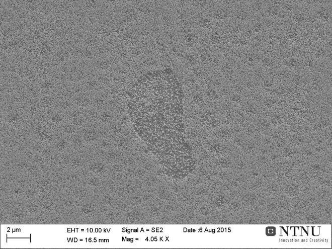
I will show the “giant” foot step mark I found in my sample during measurement using scanning electron microscope. I am not quite sure why there is suppressed growth on these area and I can find quite a lot structure similar like these actually. Many factors such as contamination or fracture can give rise to such kind of suppressed growth.

"Giant" foot step
“Giant” foot step