No nanowire growth has been done this week. Since there are two of my friends planning to use MBE with nitrogen-free chamber next week, the engineer decided to let growth chamber of MBE in the idle state or no nitrogen-related growth takes place for two-three days. Based on his experience, the decided recovery time is supposed to be sufficient enough to get nitrogen away from growth chamber, indicated from the pressure as low as 10E-10 or even lower. It means the growth chamber is in the ultra high vacuum state. The reason is because of my friends will grow in arsenic rich condition where the presence (even the small portion) of nitrogen is not desirable. Even with small portion of nitrogen, the growth sample will have diluted-nitride on it, a well-known method to alter energy band-gap of semiconductor.
No growth means characterization. I brought few of the grown samples to the scanning electron microscopy laboratory in the material department. I went training two weeks ago and did some two measurements where the results are not well-adjusted, according to my friends who has expertise in this area. In order to fix my weakness, I asked them, not once but twice to come with me but of course with different persons as I know they have their own work. Well, I think my efforts are fruitful in the sense of achieved better resolution image resulted from less distortion from astigmatism, focus and aperture optimization. Some tips and tricks were given to me , such as finding the beam location, the proper working distance (it is not in-lens type), in-plane and out-plane stage rotation.
I learned scanning-tunneling electron microscopy in Nanolab. It is bit different than the one in the material department where a transmission can be done in the same machine. Of course there is a dedicated machine to do transmission electron microscopy. As a result, such a small sample is required before it is loaded into the sample holder. I am impressed with this machine because it has way much faster venting and pumping time owing to the small chamber volume compared to the scanning electron microscopy in the material department. One of my friend always jokes that in order to get the machine in high vacuum, the user has to pay 75-100 NOK. In addition, scanning-tunneling electron microscopy in the Nanolab uses in-lens objective lens meaning the users do not have to bother much adjusting working distance as this parameter is the fixed value. With this type of lens, the resolution can go down to 0.5 nm but the drawback is located in the very limited sample size. Overall, both machine has similarities.
To use this wonderful machine, there is a theory, practical, self-training and examination part that I had to participate and pass. Generally, I did not have any difficulty in adapting with this machine. Just… The way of removing and inserting the sample holder is new for me. I have to rotate a bit, pull, rotate all the way, pull again, press “Air” button. The same method with opposite direction when I have to put it back. In one occasion of inserting the sample holder, after “Vac” button was press, I forgot to wait until the LED blink. I just force it to rotate and as a result, an alarm was beeping >_< I just realized my mistake after 5 minutes :p During this time, I was really afraid that I broke the machine XD
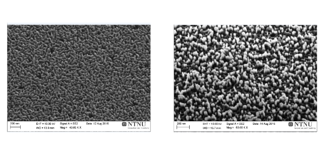
I showed my scanning electron microscopy images to the one who assisted me growing the first 7 samples. I suggested that no nanowire was observed in these samples, even with the help of AlN buffer layer. Before meeting with him, I knew that he would be disappointed with these results. Surprisingly, he did not show that sign at all and said that those short things were actually the nanowire, especially his own growth! Well, those words are in fact what I needed for the efforts we have put in the first attempts of GaN nanowire growing. Though they were not properly forming as a nanowire due to its short length. He suggested that the next growth with higher nitrogen flow. I am thinking to grow with much longer time, probably 2-3 times than what I did in the last 7 samples.
As for the last growth, I used double Ga flux rate to confirm whether the nanowire will increase its height by double. It did not turn to the expectation. It had the same height approximately with the the others. Of course, as the Ga flux was doubled, the physical mechanism on GaN nanowire formation was slightly changed. For instance, the edge has more two dimension growth (see picture below) resulting in higher non-uniformity toward the center. What a bad sample unfortunately, but I learned something at least. Maybe a lower growth rate can be planned as well? Such extreme growth rate was done by Galopin et al, almost half of the assigned Ga flux rate I set.
